SK Hynix Inc is ramping up its spending on advanced chip packaging, in hopes of capturing more of the burgeoning demand for a crucial component in artificial intelligence (AI) development: high-bandwidth memory (HBM).
The Icheon-based firm is investing more than US$1 billion in South Korea this year to expand and improve the final steps of its chip manufacture, said Lee Kang-wook, a former Samsung Electronics Co engineer who now heads up packaging development at SK Hynix.
Lee specializes in advanced ways of combining and connecting semiconductors, which has grown in importance with the advent of modern AI and its digestion of vast troves of data via parallel processing chains. While SK Hynix has not disclosed its capital expenditure budget for this year, the average analyst estimate puts the figure at 14 trillion won (US$10.5 billion). That suggests advanced packaging, which could take up a 10th of that, is a major priority.
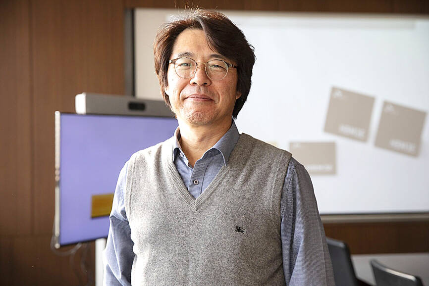
Photo: Bloomberg
“The first 50 years of the semiconductor industry has been about the front-end,” or the design and fabrication of the chips themselves, Lee said in an interview. “But the next 50 years is going to be all about the back-end,” or packaging.
Being first to achieve the next milestone in this race could now catapult companies into industry-leading positions. SK Hynix was chosen by Nvidia Corp to provide the HBM for its standard-setting AI accelerators, pushing the South Korean firm’s value up to 119 trillion won. Its stock gained about 1 percent in Seoul on Thursday, adding to a nearly 120 percent increase since the start of last year. It is now South Korea’s second most valuable company, outperforming Samsung and US rival Micron Technology Inc.
Lee, now 55 years old, helped pioneer a novel method to packaging the third generation of the technology, HBM2E, which was quickly followed by the other two major makers. That innovation was central to SK Hynix winning Nvidia as a customer in late 2019.
HBM is a type of high-performance memory that stacks chips on top of one another and connects them with through-silicon via (TSV) technology for faster and more energy-efficient data processing.
ChatGPT’s release in November 2022 was the moment Lee had been waiting for. By that time, his team had developed a new packaging method called mass reflow-molded underfill (MR-MUF), aided by his contacts in Japan. The process, which involves injecting and then hardening liquid material between layers of silicon, improved heat dissipation and production yields. SK Hynix teamed up with Namics Corp in Japan for the material and a related patent, a person familiar with the matter said.
SK Hynix is pouring the bulk of its new investment into advancing MR-MUF and TSV technologies, Lee said.
Samsung, which has for years been distracted by a succession saga at its very top, is now fighting back. Nvidia last year gave the nod to Samsung’s HBM chips, and the Suwon-based company said on Feb. 26 that it has developed the fifth generation of the technology, HBM3E, with 12 layers of DRAM chips and the industry’s largest capacity of 36 gigabytes.
On the same day, Boise, Idaho-based Micron surprised industry watchers by saying it had begun volume production of 24GB, eight-layer HBM3E, which would be part of Nvidia’s H200 Tensor Core units shipping in the second quarter.
With its big commitment to expanding and enhancing technology at home and a multibillion-dollar advanced packaging facility planned for the US, Lee remains bullish about SK Hynix’s prospects in the face of intensifying competition. He sees the present investment as laying the groundwork to meet more demand to come with future generations of HBM.
Intel Corp chief executive officer Lip-Bu Tan (陳立武) is expected to meet with Taiwanese suppliers next month in conjunction with the opening of the Computex Taipei trade show, supply chain sources said on Monday. The visit, the first for Tan to Taiwan since assuming his new post last month, would be aimed at enhancing Intel’s ties with suppliers in Taiwan as he attempts to help turn around the struggling US chipmaker, the sources said. Tan is to hold a banquet to celebrate Intel’s 40-year presence in Taiwan before Computex opens on May 20 and invite dozens of Taiwanese suppliers to exchange views

Application-specific integrated circuit designer Faraday Technology Corp (智原) yesterday said that although revenue this quarter would decline 30 percent from last quarter, it retained its full-year forecast of revenue growth of 100 percent. The company attributed the quarterly drop to a slowdown in customers’ production of chips using Faraday’s advanced packaging technology. The company is still confident about its revenue growth this year, given its strong “design-win” — or the projects it won to help customers design their chips, Faraday president Steve Wang (王國雍) told an online earnings conference. “The design-win this year is better than we expected. We believe we will win

Chizuko Kimura has become the first female sushi chef in the world to win a Michelin star, fulfilling a promise she made to her dying husband to continue his legacy. The 54-year-old Japanese chef regained the Michelin star her late husband, Shunei Kimura, won three years ago for their Sushi Shunei restaurant in Paris. For Shunei Kimura, the star was a dream come true. However, the joy was short-lived. He died from cancer just three months later in June 2022. He was 65. The following year, the restaurant in the heart of Montmartre lost its star rating. Chizuko Kimura insisted that the new star is still down

While China’s leaders use their economic and political might to fight US President Donald Trump’s trade war “to the end,” its army of social media soldiers are embarking on a more humorous campaign online. Trump’s tariff blitz has seen Washington and Beijing impose eye-watering duties on imports from the other, fanning a standoff between the economic superpowers that has sparked global recession fears and sent markets into a tailspin. Trump says his policy is a response to years of being “ripped off” by other countries and aims to bring manufacturing to the US, forcing companies to employ US workers. However, China’s online warriors