Japanese Prime Minister Fumio Kishida’s ambitious ¥4 trillion (US$26.64 billion) spending spree to revive the nation’s semiconductor industry also aims to help reorient the economy back to a positive growth cycle sought by the government and central bank.
Already there is anecdotal evidence emerging from the northern island of Hokkaido and from Kumamoto in the south that the new chip projects are starting to impact the local economies and stem the tide of people flocking to Tokyo for better jobs and schooling.
Yuto Oikawa, a realtor in Chitose, Hokkaido, cannot keep up with calls as the city transforms from a backwater to one of the nation’s hottest real-estate markets thanks to the construction of a ¥2 trillion semiconductor foundry subsidized by Kishida’s chip plan.

Photo: Bloomberg
“We are completely short-handed,” said Oikawa, 32. “It’s blown me away.”
The foundry is part of government-backed Rapidus Corp’s plan to make a giant leap in chip technology and re-establish Japan at the forefront of semiconductor expertise.
Kishida calls chips “a driving force” to help lead Japan out of its deflationary malaise of sluggish growth once and for all. A boost to wages is seen as critical to the Bank of Japan scrapping its negative interest rate, as is widely expected next month or in April, and to further increases after that.
“I hope the chip industry will take a lead on pay hikes in regional economies,” Kishida said in a video message at a chip expo in December last year. “The Japanese government will continue to give its full support to investment in the mass production of chips in our country.”
The hope is that the latest chip strategy would help fill an economic void left by the legions of companies that shifted production abroad when the yen was about twice its current strength more than a decade ago. That hollowing out of industry drained communities of spending power and employment opportunities, prompting many young people to leave.
Yet success is not guaranteed. The 2012 bankruptcy of Elpida Memory, a government-backed maker of DRAM memory chips, shows that an initial interventionist hand from the public sector can still end in failure.
Dai-Ichi Life Research Institute executive economist Hideo Kumano said that the global competitiveness of the chip industry means the latest strategy is far from certain of success.
“These subsidies are massive, but as fiscal stimulus measures, it’s possible they don’t end up paying off in the long run,” Kumano said.
The wave of people heading to the cities has resulted in four key urban areas surrounding Tokyo, Nagoya, Osaka and Fukuoka accounting for about 54 percent of Japan’s population and 60 percent of national output. From 2000 to 2020, the number of people living in Tokyo rose 16 percent, while the national population shrank.
The combined number of residents in Hokkaido and Kumamoto fell 7.7 percent during that period, while the size of their combined regional economies contracted 2.9 percent. The cheap yen has invited a wave of tourists to Japan, helping bring money into regions with sightseeing hotspots, but more needs to be done for areas off the beaten track.
The main goal of the Japanese government’s chip strategy is to triple domestic chip sales to about ¥15 trillion by 2030 and regain ground lost to Taiwanese and South Korean rivals.
The government’s spending spree to fund projects across Japan has already attracted foreign companies, such as the world’s biggest chipmaker Taiwan Semiconductor Manufacturing Co (TSMC, 台積電).
The Taiwanese giant has two factory projects in Kumamoto and there is talk of another to come. Kishida has highlighted the impact on the local community, as TSMC bumps starting salaries 20 percent above the national Japanese average.
The plant would generate an overall economic impact of ¥7 trillion and more than 10,000 jobs, Kyushu Financial Group Inc said, with an even bigger boost expected from the second TSMC foundry.

GROWING OWINGS: While Luxembourg and China swapped the top three spots, the US continued to be the largest exposure for Taiwan for the 41st consecutive quarter The US remained the largest debtor nation to Taiwan’s banking sector for the 41st consecutive quarter at the end of September, after local banks’ exposure to the US market rose more than 2 percent from three months earlier, the central bank said. Exposure to the US increased to US$198.896 billion, up US$4.026 billion, or 2.07 percent, from US$194.87 billion in the previous quarter, data released by the central bank showed on Friday. Of the increase, about US$1.4 billion came from banks’ investments in securitized products and interbank loans in the US, while another US$2.6 billion stemmed from trust assets, including mutual funds,

Micron Memory Taiwan Co (台灣美光), a subsidiary of US memorychip maker Micron Technology Inc, has been granted a NT$4.7 billion (US$149.5 million) subsidy under the Ministry of Economic Affairs A+ Corporate Innovation and R&D Enhancement program, the ministry said yesterday. The US memorychip maker’s program aims to back the development of high-performance and high-bandwidth memory chips with a total budget of NT$11.75 billion, the ministry said. Aside from the government funding, Micron is to inject the remaining investment of NT$7.06 billion as the company applied to participate the government’s Global Innovation Partnership Program to deepen technology cooperation, a ministry official told the
Taiwan Semiconductor Manufacturing Co (TSMC, 台積電), the world’s leading advanced chipmaker, officially began volume production of its 2-nanometer chips in the fourth quarter of this year, according to a recent update on the company’s Web site. The low-key announcement confirms that TSMC, the go-to chipmaker for artificial intelligence (AI) hardware providers Nvidia Corp and iPhone maker Apple Inc, met its original roadmap for the next-generation technology. Production is currently centered at Fab 22 in Kaohsiung, utilizing the company’s first-generation nanosheet transistor technology. The new architecture achieves “full-node strides in performance and power consumption,” TSMC said. The company described the 2nm process as
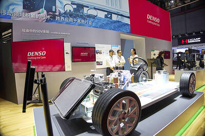
JOINT EFFORTS: MediaTek would partner with Denso to develop custom chips to support the car-part specialist company’s driver-assist systems in an expanding market MediaTek Inc (聯發科), the world’s largest mobile phone chip designer, yesterday said it is working closely with Japan’s Denso Corp to build a custom automotive system-on-chip (SoC) solution tailored for advanced driver-assistance systems and cockpit systems, adding another customer to its new application-specific IC (ASIC) business. This effort merges Denso’s automotive-grade safety expertise and deep vehicle integration with MediaTek’s technologies cultivated through the development of Media- Tek’s Dimensity AX, leveraging efficient, high-performance SoCs and artificial intelligence (AI) capabilities to offer a scalable, production-ready platform for next-generation driver assistance, the company said in a statement yesterday. “Through this collaboration, we are bringing two