Taiwan Semiconductor Manufacturing Co (TSMC, 台積電) is expected to move in the first piece of manufacturing equipment for its first 2-nanometer fab in April, paving the way for the world’s biggest contract chipmaker to start producing 2-nanometer chips in 2025, Hsinchu Science Park (新竹科學園區) Bureau director-general Wayne Wang (王永壯) yesterday said.
TSMC’s 2-nanometer fab is in Hsinchu County’s Baoshan Township (寶山), where the science park administration is working on a second-phase development program, after it completes its first-phase program, where it houses TSMC’s new research and development center, Wang said during a ceremony celebrating the science park’s 43rd anniversary.
The infrastructure construction is proceeding smoothly, he said.
Photo: Reuters, Ann Wang
TSMC’s new 2-nanometer fab construction progress, as Wang described it, indicates that TSMC might be on track to start engineering a pilot run for its 2-nanometer technology next year, before entering a production pilot run and volume production in 2025. The chipmaker said in May that it planned to start building a second 2-nanometer fab next year in Taichung.
However, Taichung Mayor Lu Shiow-yen (盧秀燕) told reporters earlier this week that TSMC could change its mind and consider building a more advanced 1.4-nanometer fab in Taichung, as the chipmaker suffered a setback in securing land to build a 1.4-nanometer fab in the Longtan (龍潭) section of Hsinchu Science Park, amid local protests over government appropriation of privately owned land for industrial use.
TSMC did not comment on whether it has altered its new fab construction plan in Taichung.
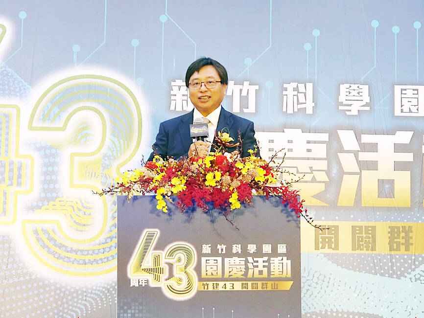
Photo: CNA
Separately, Wang told reporters that the production value of manufacturers in Hsinchu Science Park is set to recover to its peak level starting from next year, following a tough period this year when an economic slowdown and geopolitical tensions cut production value by 19 percent annually in the first half of this year to NT$668.4 billion (US$21.38 billion).
As demand returns, the decline has shrunk to about 10 percent, Wang said. He expects the recovery to extend into 2025, fueling explosive growth in production value to a new record high from companies in the park.
Additionally, the science park bureau said that the third building of the biological technology district within the science park would be completed in the second quarter of next year. It cost more than NT$3 billion, it said.
In addition, the first building of the “X” base is to be completed in the near future, Wang said.
The “X” base is designed to be a hub for the development of emerging technologies such as precision healthcare and generative artificial intelligence.
TAKING STOCK: A Taiwanese cookware firm in Vietnam urged customers to assess inventory or place orders early so shipments can reach the US while tariffs are paused Taiwanese businesses in Vietnam are exploring alternatives after the White House imposed a 46 percent import duty on Vietnamese goods, following US President Donald Trump’s announcement of “reciprocal” tariffs on the US’ trading partners. Lo Shih-liang (羅世良), chairman of Brico Industry Co (裕茂工業), a Taiwanese company that manufactures cast iron cookware and stove components in Vietnam, said that more than 40 percent of his business was tied to the US market, describing the constant US policy shifts as an emotional roller coaster. “I work during the day and stay up all night watching the news. I’ve been following US news until 3am
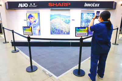
UNCERTAINTY: Innolux activated a stringent supply chain management mechanism, as it did during the COVID-19 pandemic, to ensure optimal inventory levels for customers Flat-panel display makers AUO Corp (友達) and Innolux Corp (群創) yesterday said that about 12 to 20 percent of their display business is at risk of potential US tariffs and that they would relocate production or shipment destinations to mitigate the levies’ effects. US tariffs would have a direct impact of US$200 million on AUO’s revenue, company chairman Paul Peng (彭雙浪) told reporters on the sidelines of the Touch Taiwan trade show in Taipei yesterday. That would make up about 12 percent of the company’s overall revenue. To cope with the tariff uncertainty, AUO plans to allocate its production to manufacturing facilities in
Six years ago, LVMH’s billionaire CEO Bernard Arnault and US President Donald Trump cut the blue ribbon on a factory in rural Texas that would make designer handbags for Louis Vuitton, one of the world’s best-known luxury brands. However, since the high-profile opening, the factory has faced a host of problems limiting production, 11 former Louis Vuitton employees said. The site has consistently ranked among the worst-performing for Louis Vuitton globally, “significantly” underperforming other facilities, said three former Louis Vuitton workers and a senior industry source, who cited internal rankings shared with staff. The plant’s problems — which have not
TARIFF CONCERNS: The chipmaker cited global uncertainty from US tariffs and a weakening economic outlook, but said its Singapore expansion remains on track Vanguard International Semiconductor Corp (世界先進), a foundry service provider specializing in producing power management and display driver chips, yesterday withdrew its full-year revenue projection of moderate growth for this year, as escalating US tariff tensions raised uncertainty and concern about a potential economic recession. The Hsinchu-based chipmaker in February said revenues this year would grow mildly from last year based on improving supply chain inventory levels and market demand. At the time, it also anticipated gradual quarter revenue growth. However, the US’ sweeping tariff policy has upended the industry’s supply chains and weakened economic prospects for the world economy, it said. “Now