LCD panel maker AUO Corp (友達) yesterday said it plans to convert an older-generation LCD fab in Taoyuan’s Longtan District (龍潭) into a microLED panel production site in preparation for rapid uptake of the new display technology in 2025.
The Longtan plant, dubbed Fab 5A, makes notebook computer panels, AUO said, adding that it would allocate 8.5-generation production capacity for notebook computer panels.
“MicroLED technology is highly linked to the front-end process of LCD technology, so we are preparing to upgrade an existing plant to produce the next-generation display technology,” AUO chief executive officer Frank Ko (柯富仁) told a media briefing in Taipei.
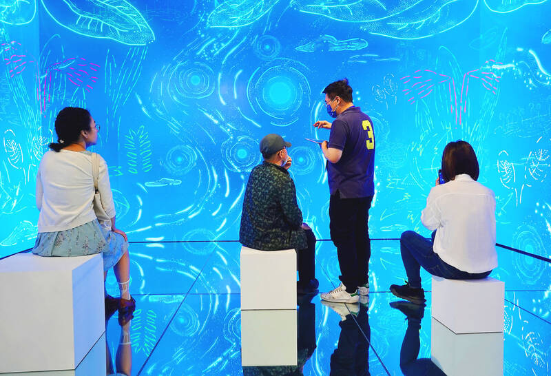
Photo: CNA
“The 5A fab and other factories in Longtan would be part of our future deployment of next-generation display technology,” Ko said.
AUO started converting its production lines in Longtan about two years ago.
The company’s microLED technology is to enter mass production in the second half of this year, it said.
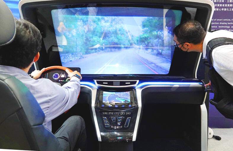
Photo: CNA
That would make it one of two panel makers in the world capable of producing microLED panels this year, joining Samsung Electronics Co of South Korea.
AUO’s first microLED panels would be 1.39-inch panels used in smartwatches, it said.
Bigger panels used in TVs and public information displays would be available next year, it said.
The microLED panels would also be used in vehicle displays such as central information displays and smart cockpits, with mass production scheduled for 2025 or 2026 due to longer certification periods, AUO said.
As more companies join the microLED supply chain, AUO expects manufacturing costs to drop 50 percent every two years, a rule similar to Moore’s law in the semiconductor industry, AUO chairman Paul Peng (彭?浪) said.
Fairchild Semiconductor International Inc and Intel Corp founder Gordon Moore in 1965 said that the number of transistors in an IC doubles about every two years.
AUO said it estimates that the manufacturing cost of microLED panels would reach a sweet spot in 2025.
Mini LED panels remain much more pricey than their LCD counterparts, it said.
AUO allocates about 30 percent of its 2,000 research engineers for the development of the next-generation display technology to deliver higher resolution and better color performance than LCD technology, it said.
Separately, Innolux Corp (群創) said it is working with customers to develop microLED panels, without saying when it is to deliver its first such product.
The company said it is considering converting a 5.5-generation LCD fab to a microLED panel production base.
Other options include using the capacity to produce niche products, displays used in 5G or 6G devices or antenna for communicating with low Earth orbit satellites, Innolux said.
The 5.5-generation fab is entering a “green” idle state as the company phases out some commodity products, Innolux chairman Jim Hung (洪進揚) said.
The company is adjusting its manufacturing capacity for products with better margins and has transformed a 3.5-generation fab into a production site for advanced chip packaging technology, the company said.
Innolux also uses a 4-generation LCD manufacturing fab to produce X-ray sensors and a 4.5-generation fab to make e-paper displays, the company added.
The company said it expects to launch a project with Vedanta Group in June after receiving Indian government approval for subsidies.
Innolux has signed an agreement with Vedanta to help the Mumbai-based firm build a flat-panel production line in India and help license its intellectual property.
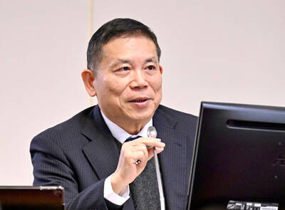
Taiwan will prioritize the development of silicon photonics by taking advantage of its strength in the semiconductor industry to build another shield to protect the local economy, National Development Council (NDC) Minister Paul Liu (劉鏡清) said yesterday. Speaking at a meeting of the legislature’s Economics Committee, Liu said Taiwan already has the artificial intelligence (AI) industry as a shield, after the semiconductor industry, to safeguard the country, and is looking at new unique fields to build more economic shields. While Taiwan will further strengthen its existing shields, over the longer term, the country is determined to focus on such potential segments as
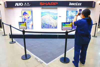
UNCERTAINTY: Innolux activated a stringent supply chain management mechanism, as it did during the COVID-19 pandemic, to ensure optimal inventory levels for customers Flat-panel display makers AUO Corp (友達) and Innolux Corp (群創) yesterday said that about 12 to 20 percent of their display business is at risk of potential US tariffs and that they would relocate production or shipment destinations to mitigate the levies’ effects. US tariffs would have a direct impact of US$200 million on AUO’s revenue, company chairman Paul Peng (彭雙浪) told reporters on the sidelines of the Touch Taiwan trade show in Taipei yesterday. That would make up about 12 percent of the company’s overall revenue. To cope with the tariff uncertainty, AUO plans to allocate its production to manufacturing facilities in
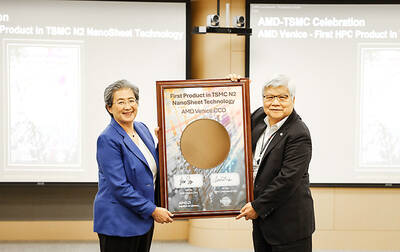
COLLABORATION: Given Taiwan’s key position in global supply chains, the US firm is discussing strategies with local partners and clients to deal with global uncertainties Advanced Micro Devices Inc (AMD) yesterday said it is meeting with local ecosystem partners, including Taiwan Semiconductor Manufacturing Co (TSMC, 台積電), to discuss strategies, including long-term manufacturing, to navigate uncertainties such as US tariffs, as Taiwan occupies an important position in global supply chains. AMD chief executive officer Lisa Su (蘇姿丰) told reporters that Taiwan is an important part of the chip designer’s ecosystem and she is discussing with partners and customers in Taiwan to forge strong collaborations on different areas during this critical period. AMD has just become the first artificial-intelligence (AI) server chip customer of TSMC to utilize its advanced
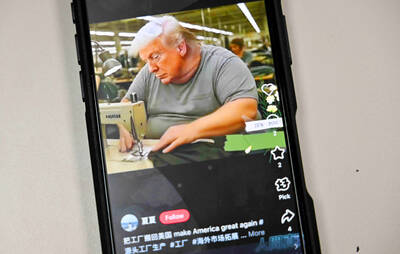
While China’s leaders use their economic and political might to fight US President Donald Trump’s trade war “to the end,” its army of social media soldiers are embarking on a more humorous campaign online. Trump’s tariff blitz has seen Washington and Beijing impose eye-watering duties on imports from the other, fanning a standoff between the economic superpowers that has sparked global recession fears and sent markets into a tailspin. Trump says his policy is a response to years of being “ripped off” by other countries and aims to bring manufacturing to the US, forcing companies to employ US workers. However, China’s online warriors