Taiwan Semiconductor Manufacturing Co (TSMC, 台積電) on Saturday said that it would hold a ceremony on Thursday to mark the beginning of mass production using its 3-nanometer process.
The company is to mark the placing of the final beam at its Fab 18 in the Southern Taiwan Science Park (南部科學園區) in Tainan.
It would also detail its plans for expanding 3-nanometer production at the facility in the coming years, TSMC said.

Photo: Lam Yik Fei, Bloomberg
The fab currently mass produces chips using the 5-nanometer process.
It is unusual for TSMC to hold a ceremony to mark the beginning of commercial production of a new technology.
Analysts have said that the ceremony aims to announce TSMC’s intention to continue using Taiwan as a hub for research and development (R&D) and production, despite its overseas investments.
Speculation has risen that the company could relocate its production and R&D centers to the US.
The rumors arose after TSMC on Dec. 6 said at a tool-in ceremony for its 12-inch wafer plant in Phoenix, Arizona, that it would increase its planned US$12 billion investment there to US$40 billion to build a 3-nanometer fab by 2026, in addition to its planned 4-nanometer plant due to be completed in 2024.
The concerns intensified after TSMC sent a large group of Taiwanese engineers to support the Arizona plant, raising investors’ fears that the move could undermine the firm’s base in Taiwan.
The planned Arizona plants are expected to produce more than 600,000 wafers a year, TSMC has said.
Last week, TSMC chief executive officer C.C. Wei (魏哲家) told a forum held by the Mount Jade Global Science and Technology Association in Taipei that there was “no chance” that a single wafer fab would give a location a technical advantage over other semiconductor manufacturing sites.
TSMC plans to start mass producing chips using the N3E process next year. The process is based on the 3-nanometer technology and produces more efficient chips with a better yield rate.
The company is also developing a more sophisticated 2-nanometer process and plans to build a 2-nanometer fab in Hsinchu, with mass production scheduled to begin in 2025.
The 3-nanometer process uses 16-nanometer fin field-effect transistor technology, which is a 3D transistor structure that allows a chip to run faster using the same amount of energy or to run at the same speed on reduced power.
Chips made using the technology are 10 to 15 percent faster and 25 to 30 percent more energy-efficient than those produced with the 5-nanometer process, whose mass production started last year.
Apple Inc and Intel Corp are expected to place orders for chips made with TSMC’s 3-nanometer process, analysts have said.
The 2-nanometer process would be the first technology in which TSMC employs a gate-all-around structure, which reduces undesirable variability and mobility loss, making the technology the most competitive and efficient on the market, the company has said.
Early this month, Wayne Wang (王永壯), director general of the Hsinchu Science Park Bureau, said TSMC has plans to build a 1-nanometer process fab in the Longtan (龍潭) section of the Hsinchu Science Park (新竹科學園區).
TSMC has yet to confirm Wang’s announcement.
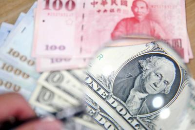
The US dollar was trading at NT$29.7 at 10am today on the Taipei Foreign Exchange, as the New Taiwan dollar gained NT$1.364 from the previous close last week. The NT dollar continued to rise today, after surging 3.07 percent on Friday. After opening at NT$30.91, the NT dollar gained more than NT$1 in just 15 minutes, briefly passing the NT$30 mark. Before the US Department of the Treasury's semi-annual currency report came out, expectations that the NT dollar would keep rising were already building. The NT dollar on Friday closed at NT$31.064, up by NT$0.953 — a 3.07 percent single-day gain. Today,

‘SHORT TERM’: The local currency would likely remain strong in the near term, driven by anticipated US trade pressure, capital inflows and expectations of a US Fed rate cut The US dollar is expected to fall below NT$30 in the near term, as traders anticipate increased pressure from Washington for Taiwan to allow the New Taiwan dollar to appreciate, Cathay United Bank (國泰世華銀行) chief economist Lin Chi-chao (林啟超) said. Following a sharp drop in the greenback against the NT dollar on Friday, Lin told the Central News Agency that the local currency is likely to remain strong in the short term, driven in part by market psychology surrounding anticipated US policy pressure. On Friday, the US dollar fell NT$0.953, or 3.07 percent, closing at NT$31.064 — its lowest level since Jan.
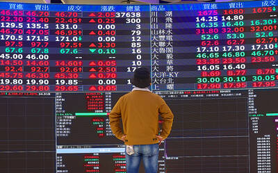
The New Taiwan dollar and Taiwanese stocks surged on signs that trade tensions between the world’s top two economies might start easing and as US tech earnings boosted the outlook of the nation’s semiconductor exports. The NT dollar strengthened as much as 3.8 percent versus the US dollar to 30.815, the biggest intraday gain since January 2011, closing at NT$31.064. The benchmark TAIEX jumped 2.73 percent to outperform the region’s equity gauges. Outlook for global trade improved after China said it is assessing possible trade talks with the US, providing a boost for the nation’s currency and shares. As the NT dollar

The Financial Supervisory Commission (FSC) yesterday met with some of the nation’s largest insurance companies as a skyrocketing New Taiwan dollar piles pressure on their hundreds of billions of dollars in US bond investments. The commission has asked some life insurance firms, among the biggest Asian holders of US debt, to discuss how the rapidly strengthening NT dollar has impacted their operations, people familiar with the matter said. The meeting took place as the NT dollar jumped as much as 5 percent yesterday, its biggest intraday gain in more than three decades. The local currency surged as exporters rushed to