The US is tightening restrictions on China’s access to chipmaking gear, two major equipment suppliers have said, underscoring Washington’s accelerating efforts to curb Beijing’s economic ambitions.
Washington had banned the sale of most gear that can fabricate chips of 10 nanometers or better to Chinese firm Semiconductor Manufacturing International Corp (SMIC, 中芯國際) without a license.
Now it has expanded that barrier to equipment that can make anything more advanced than 14 nanometers, Lam Research Corp chief executive officer Tim Archer told analysts.
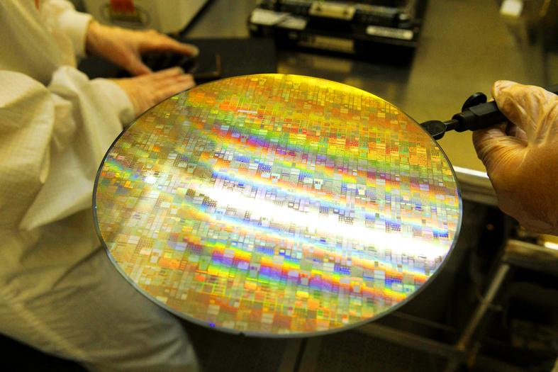
Photo: Bloomberg
The moratorium likely extends beyond SMIC and includes other fabrication plants run by contract chipmakers operating in China, including those by Taiwan Semiconductor Manufacturing Co (TSMC, 台積電).
“We were recently notified that there was to be a broadening of the restrictions of technology shipments to China for fabs that are operating below 14 nanometers,” Archer said during a conference call on Wednesday. “That’s the change, I think, people have been thinking might be coming and we’re prepared to fully comply. We’re working with the US government.”
In chip manufacturing, production identified by lower numbers of nanometers is more advanced. That means raising the restriction level to 14 nanometers would cover a broader range of semiconductor equipment.
The US Department of Commerce said in a statement that the administration of US President Joe Biden is tightening policies aimed at the People’s Republic of China (PRC), without specifying the precise chip geometry.
“The Biden administration is focused on impairing PRC efforts to manufacture advanced semiconductors to address significant national security risks to the United States,” the agency said.
All US equipment makers have in the past few weeks received letters from the commerce department telling them not to supply gear to Chinese firms for manufacturing at 14 nanometers or below, people familiar with the matter said.
The letters are at least partly an effort by the Biden administration to look tough on China, but the department had already declined many licenses at 14 nanometers so the change would have little financial effects, they said.
The new requirements are targeted at foundries — facilities making logic chips for others — and exclude memory chips “to the best of our understanding,” Archer said.
Lam Research executives said they had incorporated the expected effects of the US requirements into their outlook for the third quarter of this year, without elaborating.
KLA Corp CEO Rick Wallace on Thursday confirmed that his company had been notified by the US government of the change in export licensing requirements on China-bound gear for chips more advanced than 14 nanometers.
Wallace said there was no material impact on KLA’s business.
The comments from the two California-based companies mark the first detailed confirmation that the Biden administration is ramping up attempts to contain China. The US is pushing partner countries such as the Netherlands and Japan to ban ASML Holding NV and Nikon Corp from selling mainstream technology essential in making a large chunk of the world’s chips to China.
The new rules cover a wider swath of semiconductors across a plethora of industries and possibly affect far more companies than standing restrictions targeted at SMIC. While the new curbs specifically cover equipment capable of making chips more advanced than 14 nanometers, mature chips could still be affected, as about 90 percent of gear is compatible from one generation to the next. Semiconductor manufacturers can reuse equipment as they migrate to more sophisticated nodes, meaning a ban on one generation could have longer-term ripple effects.
SMIC’s most sophisticated technology is 14 nanometers, while the best TSMC uses in China is 16 nanometers. Those are three generations behind the most cutting-edge technology TSMC uses in Taiwan.
The new rules are likely to affect SMIC, TSMC and any others with the ambition to build capacity for relatively advanced chips in China, as well as gear makers such as Applied Materials Inc, ASML and Tokyo Electron Ltd, which sell to the world’s largest chip market.

Intel Corp chief executive officer Lip-Bu Tan (陳立武) is expected to meet with Taiwanese suppliers next month in conjunction with the opening of the Computex Taipei trade show, supply chain sources said on Monday. The visit, the first for Tan to Taiwan since assuming his new post last month, would be aimed at enhancing Intel’s ties with suppliers in Taiwan as he attempts to help turn around the struggling US chipmaker, the sources said. Tan is to hold a banquet to celebrate Intel’s 40-year presence in Taiwan before Computex opens on May 20 and invite dozens of Taiwanese suppliers to exchange views

Application-specific integrated circuit designer Faraday Technology Corp (智原) yesterday said that although revenue this quarter would decline 30 percent from last quarter, it retained its full-year forecast of revenue growth of 100 percent. The company attributed the quarterly drop to a slowdown in customers’ production of chips using Faraday’s advanced packaging technology. The company is still confident about its revenue growth this year, given its strong “design-win” — or the projects it won to help customers design their chips, Faraday president Steve Wang (王國雍) told an online earnings conference. “The design-win this year is better than we expected. We believe we will win

Chizuko Kimura has become the first female sushi chef in the world to win a Michelin star, fulfilling a promise she made to her dying husband to continue his legacy. The 54-year-old Japanese chef regained the Michelin star her late husband, Shunei Kimura, won three years ago for their Sushi Shunei restaurant in Paris. For Shunei Kimura, the star was a dream come true. However, the joy was short-lived. He died from cancer just three months later in June 2022. He was 65. The following year, the restaurant in the heart of Montmartre lost its star rating. Chizuko Kimura insisted that the new star is still down
While China’s leaders use their economic and political might to fight US President Donald Trump’s trade war “to the end,” its army of social media soldiers are embarking on a more humorous campaign online. Trump’s tariff blitz has seen Washington and Beijing impose eye-watering duties on imports from the other, fanning a standoff between the economic superpowers that has sparked global recession fears and sent markets into a tailspin. Trump says his policy is a response to years of being “ripped off” by other countries and aims to bring manufacturing to the US, forcing companies to employ US workers. However, China’s online warriors