Taiwan Semiconductor Manufacturing Co (TSMC, 台積電) yesterday said its subsidiary TSMC Japan 3DIC R&D Center has completed construction of its clean room in the Tsukuba Center of the National Institute of Advanced Industrial Science and Technology.
The center was established in Japan’s Ibaraki Prefecture in March last year to pursue research into the next generations of 3D silicon stacking and advanced packaging technologies in materials science, the chipmaker said in a statement.
The Japanese government is to provide an unspecified subsidy for the center.
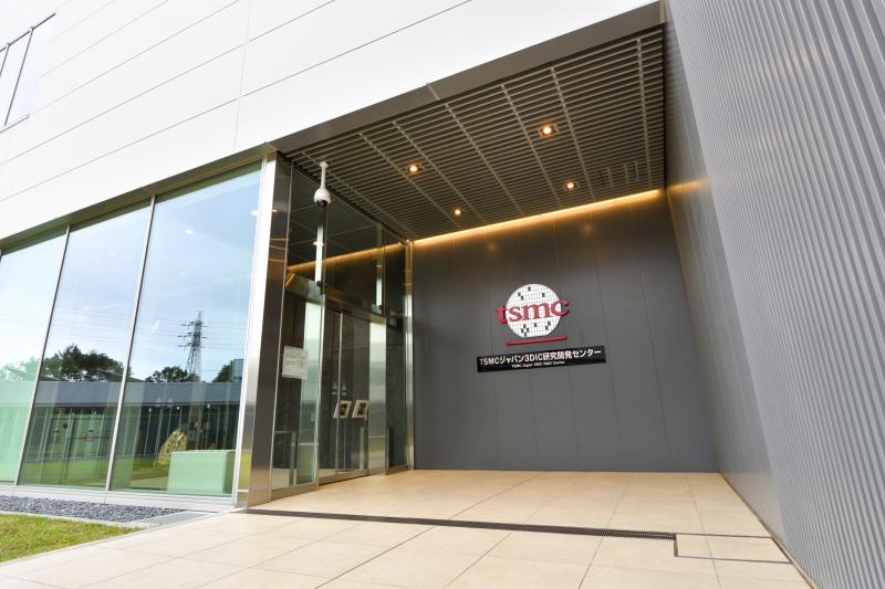
Photo courtesy of Taiwan Semiconductor Manufacturing Co
The new technologies would enable system-level innovations to enhance computing performance and integrate more functionality, opening a new path for driving semiconductor technology forward in addition to the industry’s conventional path of shrinking transistor size, TSMC said.
With the completion of the clean room, the TSMC Japan 3DIC R&D Center is to support research and development of state-of-the-art 3D IC packaging material in collaboration with its Japanese partners, domestic research institutes and universities possessing strengths in semiconductor materials and equipment, the statement said.
“Beginning with our foundry business model, TSMC has always believed that by focusing on what we do best, each of us in the semiconductor field can maximize our contribution to pushing technology forward,” TSMC chief executive C.C. Wei (魏哲家) said in the statement.
“The Japan 3DIC R&D Center is a perfect example of this collaboration in action. By bringing TSMC together with Japanese talent, we will empower each other to make breakthroughs together,” he said.
“We are witnessing an increase in structural demand driven by the megatrends of 5G and high-performance computing-related applications, and further technology innovation will be needed to meet this demand,” TSMC Japan 3DIC R&D Center vice president and general manager Yutaka Emoto said in the statement.
“Japan has many companies with functional materials and key technologies that are important in the global semiconductor supply chain, and TSMC will continue to work on semiconductor process innovation through joint research and development with them,” he said.
“At the same time, we can serve as a bridge between our partners at the 3DIC R&D Center and the world-class semiconductor companies among TSMC’s customers,” he said.
Taiwan Semiconductor Manufacturing Co (TSMC, 台積電) yesterday said that its investment plan in Arizona is going according to schedule, following a local media report claiming that the company is planning to break ground on its third wafer fab in the US in June. In a statement, TSMC said it does not comment on market speculation, but that its investments in Arizona are proceeding well. TSMC is investing more than US$65 billion in Arizona to build three advanced wafer fabs. The first one has started production using the 4-nanometer (nm) process, while the second one would start mass production using the

A TAIWAN DEAL: TSMC is in early talks to fully operate Intel’s US semiconductor factories in a deal first raised by Trump officials, but Intel’s interest is uncertain Broadcom Inc has had informal talks with its advisers about making a bid for Intel Corp’s chip-design and marketing business, the Wall Street Journal reported, citing people familiar with the matter. Nothing has been submitted to Intel and Broadcom could decide not to pursue a deal, according to the Journal. Bloomberg News earlier reported that Taiwan Semiconductor Manufacturing Co (TSMC, 台積電) is in early talks for a controlling stake in Intel’s factories at the request of officials at US President Donald Trump’s administration, as the president looks to boost US manufacturing and maintain the country’s leadership in critical technologies. Trump officials raised the
‘SILVER LINING’: Although the news caused TSMC to fall on the local market, an analyst said that as tariffs are not set to go into effect until April, there is still time for negotiations US President Donald Trump on Tuesday said that he would likely impose tariffs on semiconductor, automobile and pharmaceutical imports of about 25 percent, with an announcement coming as soon as April 2 in a move that would represent a dramatic widening of the US leader’s trade war. “I probably will tell you that on April 2, but it’ll be in the neighborhood of 25 percent,” Trump told reporters at his Mar-a-Lago club when asked about his plan for auto tariffs. Asked about similar levies on pharmaceutical drugs and semiconductors, the president said that “it’ll be 25 percent and higher, and it’ll
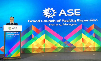
CHIP BOOM: Revenue for the semiconductor industry is set to reach US$1 trillion by 2032, opening up opportunities for the chip pacakging and testing company, it said ASE Technology Holding Co (日月光投控), the world’s largest provider of outsourced semiconductor assembly and test (OSAT) services, yesterday launched a new advanced manufacturing facility in Penang, Malaysia, aiming to meet growing demand for emerging technologies such as generative artificial intelligence (AI) applications. The US$300 million facility is a critical step in expanding ASE’s global footprint, offering an alternative for customers from the US, Europe, Japan, South Korea and China to assemble and test chips outside of Taiwan amid efforts to diversify supply chains. The plant, the company’s fifth in Malaysia, is part of a strategic expansion plan that would more than triple