The EU is considering building an advanced semiconductor factory in Europe in an attempt to avoid relying on the US and Asia for technology at the heart of some of its major industries.
The EU is exploring how to produce semiconductors with features smaller than 10 nanometers, and eventually down to 2-nanometer chips, according to people familiar with the project. The aim is to curtail dependence on countries such as Taiwan for chips to power 5G wireless systems, connected cars, high-performance computing and more.
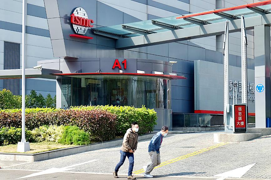
Taiwan Semiconductor Manufacturing Co (TSMC, 台積電) and Samsung Electronics Co of South Korea, the two leaders making the most innovative processors in the sector, could be involved in the EU project, but nothing has been decided, a French Finance Ministry official said in a press briefing on Thursday, following the report from Bloomberg.

Photo: Sam Yeh / AFP
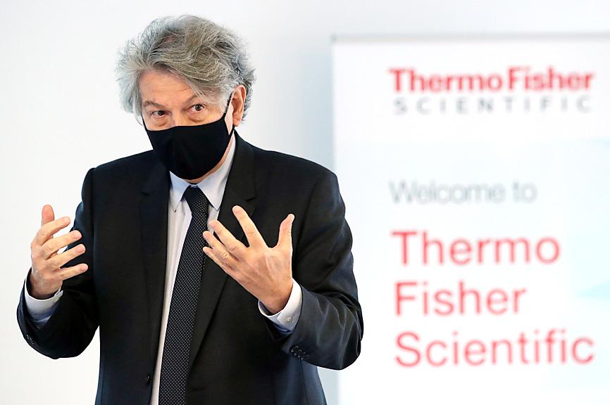
European attempts to ramp up production — led in part by European Industry Commissioner Thierry Breton — could involve redeveloping an existing foundry or building a new one, the people said, adding that no final decision has been taken and the time frame of the project is still to be determined.
“When it comes to fab location selection, we need to consider many factors including customers’ need. TSMC does not rule out any possibility, but there is no concrete plan at this time,” TSMC spokeswoman Nina Kao (高孟華) said in an e-mail when asked about cooperating with Europe.
Once a hub of semiconductor factories, Europe has dramatically cut back on manufacturing over the past 20 years, with automotive-chip designers including NXP Semiconductors NV and Infineon Technologies AG preferring to outsource a major chunk of production to giants like TSMC, and other foundries. When carmakers wanted to increase orders at the end of last year, they struggled to secure capacity, after demand had already been allocated to other industries such as smartphones.

Photo: Reuters
The EU outlined a goal last year to produce at least one-fifth of the world’s chips and microprocessors by value, without giving details on how this would be achieved.
“Without an autonomous European capacity on microelectronics, there will be no European digital sovereignty,” Breton said in a speech, adding that Europe currently accounts for less than 10 percent of global production of processors and other microelectronics.
To reach those goals, the European Commission said it would launch a European alliance on microelectronics, which will likely include Europe’s major chipmakers and possibly also carmakers and telecom companies.
Technical work is ongoing to map out a plan for the alliance, but initial discussions about the fabrication plans have already taken place, according to people familiar with the matter. The alliance is due to be formally unveiled at the end of the first quarter of the year.
Europe’s plans to reinvest in leading-edge chip fabrication may be too little, too late as China, Japan and the US all try to increase or regain their self-sufficiency in semiconductors.
But all are slipping further behind industry leaders Samsung and especially TSMC, which announced capital spending of as much as US$28 billion for this year, and the Asian companies, whose current leading-edge chips are 5nm, have plans to go down to the even more advanced 3nm, while GlobalFoundries Inc is Europe’s main foundry, which typically produces 28nm processors at its Dresden factory for mainstream applications.
The industry has also spent decades crafting a well-oiled global supply chain that would be difficult to change overnight, according to Peter Wennink, chief executive officer of ASML Holding NV of the Netherlands, which has an effective monopoly on the machines needed to fabricate the best chips. Regions will have to rebuild a local ecosystem, which in turn would likely raise costs.
“If you think that you can actually replicate that within a very short term, it’s simply not possible,” Wennink said at ASML’s full-year earnings press conference last month. “If governments are determined to do this, it will take years to break this up, and not months.”
One of the biggest hurdles for the EU’s semiconductor plans could come down to financing. At a conference last week, French Finance Minister Bruno LeMaire said Europe’s industrial projects, including on semiconductors, are all very investment intensive.
“One of the weak points is the access to risk capital in Europe and the implementation of the capital market in Europe,” he said.
Breton said last year the chip alliance would be armed with an initial combined public and private investment of as much as 30 billion euros, only slightly higher than TSMC’s annual capital expenditure this year.
Around 19 member states have already backed the commission’s plans and have agreed to establish an investment instrument co-financed by the countries and participating companies.

Taiwan will prioritize the development of silicon photonics by taking advantage of its strength in the semiconductor industry to build another shield to protect the local economy, National Development Council (NDC) Minister Paul Liu (劉鏡清) said yesterday. Speaking at a meeting of the legislature’s Economics Committee, Liu said Taiwan already has the artificial intelligence (AI) industry as a shield, after the semiconductor industry, to safeguard the country, and is looking at new unique fields to build more economic shields. While Taiwan will further strengthen its existing shields, over the longer term, the country is determined to focus on such potential segments as

UNCERTAINTY: Innolux activated a stringent supply chain management mechanism, as it did during the COVID-19 pandemic, to ensure optimal inventory levels for customers Flat-panel display makers AUO Corp (友達) and Innolux Corp (群創) yesterday said that about 12 to 20 percent of their display business is at risk of potential US tariffs and that they would relocate production or shipment destinations to mitigate the levies’ effects. US tariffs would have a direct impact of US$200 million on AUO’s revenue, company chairman Paul Peng (彭雙浪) told reporters on the sidelines of the Touch Taiwan trade show in Taipei yesterday. That would make up about 12 percent of the company’s overall revenue. To cope with the tariff uncertainty, AUO plans to allocate its production to manufacturing facilities in

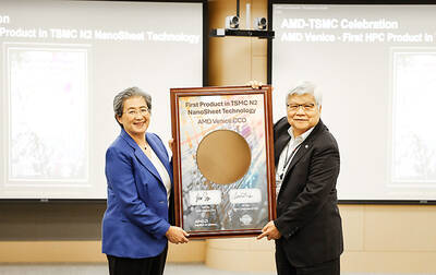
COLLABORATION: Given Taiwan’s key position in global supply chains, the US firm is discussing strategies with local partners and clients to deal with global uncertainties Advanced Micro Devices Inc (AMD) yesterday said it is meeting with local ecosystem partners, including Taiwan Semiconductor Manufacturing Co (TSMC, 台積電), to discuss strategies, including long-term manufacturing, to navigate uncertainties such as US tariffs, as Taiwan occupies an important position in global supply chains. AMD chief executive officer Lisa Su (蘇姿丰) told reporters that Taiwan is an important part of the chip designer’s ecosystem and she is discussing with partners and customers in Taiwan to forge strong collaborations on different areas during this critical period. AMD has just become the first artificial-intelligence (AI) server chip customer of TSMC to utilize its advanced

Chizuko Kimura has become the first female sushi chef in the world to win a Michelin star, fulfilling a promise she made to her dying husband to continue his legacy. The 54-year-old Japanese chef regained the Michelin star her late husband, Shunei Kimura, won three years ago for their Sushi Shunei restaurant in Paris. For Shunei Kimura, the star was a dream come true. However, the joy was short-lived. He died from cancer just three months later in June 2022. He was 65. The following year, the restaurant in the heart of Montmartre lost its star rating. Chizuko Kimura insisted that the new star is still down