A new high-end IC packaging and testing plant planned by contract chipmaker Taiwan Semiconductor Manufacturing Co (TSMC, 台積電) in Miaoli County is expected to start operations in the middle of next year, Miaoli County Commissioner Hsu Yao-chang (徐耀昌) said.
Hsu wrote on Facebook that TSMC, the world’s largest pure wafer foundry operator, would invest NT$303.2 billion (US$10.1 billion) to build the plant, the largest-ever single investment in Taiwan.
However, TSMC declined to disclose the financial terms of the deal, while a company board meeting on May 12 approved a spending plan worth NT$168.2 billion as part of its investment plans.
Construction of the plant, which is to be built in the Jhunan Township (竹南) section of the Hsinchu Science Park (新竹科學園區), is scheduled to be completed in May next year, with operations to begin a few months later, Hsu said.
The investment is expected to create more than 1,000 jobs and boost prosperity in the area, he said.
TSMC has stepped up preparations for the Jhunan investment plan and has been meeting with county government officials, with a meeting scheduled for the middle of this month to brief them on the construction work, he said.
In November last year, the company passed an environmental impact assessment conducted by the Miaoli County Government.
The plant is part of TSMC’s aggressive move into high-end IC packaging and testing services to provide one-stop shopping for chips with advanced 3D IC packaging and testing technology.
TSMC operates advanced IC packaging and testing plants in Taoyuan, Hsinchu, Taichung and Tainan.
In a separate statement, TSMC said it has launched the world’s first 7-nanometer (nm) Automotive Design Enablement Platform (ADEP), which would accelerate time-to-design for artificial intelligence inference engines, advanced driver-assistance systems and autonomous driving applications.
Following mass production of its 7nm process in 2018, the launch of ADEP demonstrates the chipmaker’s industry-leading yield learning and quality assurance experience, TSMC said.
It also enables the company to deliver on increased demand for leading-edge processes to fulfill the high computational needs of automotive applications, the company said.
“TSMC is uniquely positioned with our 7nm experience and comprehensive design ecosystem to unleash our customers’ innovations and achieve first-time silicon success while meeting the rigorous demands of bringing safer and smarter vehicles to market,” TSMC senior vice president of research and development and technology development Cliff Hou (侯永清) said in the statement.

Taiwan Semiconductor Manufacturing Co (TSMC, 台積電) yesterday said that its investment plan in Arizona is going according to schedule, following a local media report claiming that the company is planning to break ground on its third wafer fab in the US in June. In a statement, TSMC said it does not comment on market speculation, but that its investments in Arizona are proceeding well. TSMC is investing more than US$65 billion in Arizona to build three advanced wafer fabs. The first one has started production using the 4-nanometer (nm) process, while the second one would start mass production using the

‘SILVER LINING’: Although the news caused TSMC to fall on the local market, an analyst said that as tariffs are not set to go into effect until April, there is still time for negotiations US President Donald Trump on Tuesday said that he would likely impose tariffs on semiconductor, automobile and pharmaceutical imports of about 25 percent, with an announcement coming as soon as April 2 in a move that would represent a dramatic widening of the US leader’s trade war. “I probably will tell you that on April 2, but it’ll be in the neighborhood of 25 percent,” Trump told reporters at his Mar-a-Lago club when asked about his plan for auto tariffs. Asked about similar levies on pharmaceutical drugs and semiconductors, the president said that “it’ll be 25 percent and higher, and it’ll
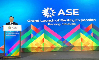
CHIP BOOM: Revenue for the semiconductor industry is set to reach US$1 trillion by 2032, opening up opportunities for the chip pacakging and testing company, it said ASE Technology Holding Co (日月光投控), the world’s largest provider of outsourced semiconductor assembly and test (OSAT) services, yesterday launched a new advanced manufacturing facility in Penang, Malaysia, aiming to meet growing demand for emerging technologies such as generative artificial intelligence (AI) applications. The US$300 million facility is a critical step in expanding ASE’s global footprint, offering an alternative for customers from the US, Europe, Japan, South Korea and China to assemble and test chips outside of Taiwan amid efforts to diversify supply chains. The plant, the company’s fifth in Malaysia, is part of a strategic expansion plan that would more than triple

When an apartment comes up for rent in Germany’s big cities, hundreds of prospective tenants often queue down the street to view it, but the acute shortage of affordable housing is getting scant attention ahead of today’s snap general election. “Housing is one of the main problems for people, but nobody talks about it, nobody takes it seriously,” said Andreas Ibel, president of Build Europe, an association representing housing developers. Migration and the sluggish economy top the list of voters’ concerns, but analysts say housing policy fails to break through as returns on investment take time to register, making the