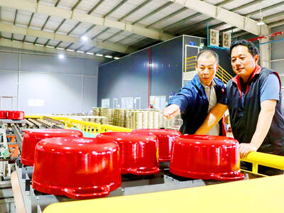
Advanced Semiconductor Engineering Inc (ASE, 日月光導體), the world’s largest chip packager and tester, on Saturday held a plaque-unveiling ceremony to launch a joint venture with Japan’s TDK Corp in Kaohsiung.
With initial capital of NT$1.5 billion (US$51.2 million), ASE Embedded Electronics Inc (日月暘電子) is to start operations in Kaohsiung’s Nantze Export Processing Zone (楠梓加工出口區), focusing on the manufacturing of integrated-circuit (IC) embedded substrates using TDK’s semiconductor embedded substrate (SESUB) technology, ASE said.
The SESUB technology enables semiconductor chips to be shrunk to 50 micrometers and embedded in a four-layer plastic substrate.
ASE Embedded — in which ASE owns 51 percent and TDK 49 percent, and which employs 150 people — is to use the technology to integrate dozens of chips into smaller and thinner spaces, eyeing an increase of semiconductor content in portable and wearable devices, ASE said.
The company first announced its joint venture with TDK in May 2015 and completed a registration with the Ministry of Economic Affairs later that year.
The two companies signed an agreement on technology transfer in 2016 and completed installing production facilities at the plant last year.
The ceremony was attended by ASE chief operating officer Tien Wu (吳田玉), ASE Embedded president Chung Chih-hsiao (鍾智孝), Export Processing Zone Administration director-general Huang Wen-guu (黃文谷), Kaohsiung Economic Development Bureau Director Tseng Wen-sheng (曾文生) and officials from the Japan-Taiwan Exchange Association’s Kaohsiung Office, ASE said.

STEEP DECLINE: Yesterday’s drop was the third-steepest in its history, the steepest being Monday’s drop in the wake of the tariff announcement on Wednesday last week Taiwanese stocks continued their heavy sell-off yesterday, as concerns over US tariffs and unwinding of leveraged bets weighed on the market. The benchmark TAIEX plunged 1,068.19 points, or 5.79 percent, to 17,391.76, notching the biggest drop among Asian peers as it hit a 15-month low. The decline came even after the government on late Tuesday authorized the NT$500 billion (US$15.2 billion) National Stabilization Fund (國安基金) to step in to buoy the market amid investors’ worries over tariffs imposed by US President Donald Trump. Yesterday’s decline was the third-steepest in its history, trailing only the declines of 2,065.87 points on Monday and
TAKING STOCK: A Taiwanese cookware firm in Vietnam urged customers to assess inventory or place orders early so shipments can reach the US while tariffs are paused Taiwanese businesses in Vietnam are exploring alternatives after the White House imposed a 46 percent import duty on Vietnamese goods, following US President Donald Trump’s announcement of “reciprocal” tariffs on the US’ trading partners. Lo Shih-liang (羅世良), chairman of Brico Industry Co (裕茂工業), a Taiwanese company that manufactures cast iron cookware and stove components in Vietnam, said that more than 40 percent of his business was tied to the US market, describing the constant US policy shifts as an emotional roller coaster. “I work during the day and stay up all night watching the news. I’ve been following US news until 3am
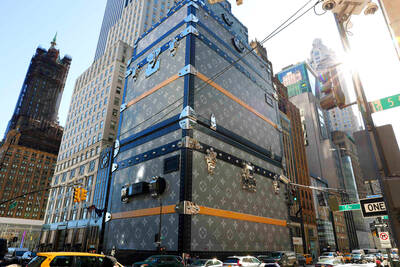
Six years ago, LVMH’s billionaire CEO Bernard Arnault and US President Donald Trump cut the blue ribbon on a factory in rural Texas that would make designer handbags for Louis Vuitton, one of the world’s best-known luxury brands. However, since the high-profile opening, the factory has faced a host of problems limiting production, 11 former Louis Vuitton employees said. The site has consistently ranked among the worst-performing for Louis Vuitton globally, “significantly” underperforming other facilities, said three former Louis Vuitton workers and a senior industry source, who cited internal rankings shared with staff. The plant’s problems — which have not
TARIFF CONCERNS: The chipmaker cited global uncertainty from US tariffs and a weakening economic outlook, but said its Singapore expansion remains on track Vanguard International Semiconductor Corp (世界先進), a foundry service provider specializing in producing power management and display driver chips, yesterday withdrew its full-year revenue projection of moderate growth for this year, as escalating US tariff tensions raised uncertainty and concern about a potential economic recession. The Hsinchu-based chipmaker in February said revenues this year would grow mildly from last year based on improving supply chain inventory levels and market demand. At the time, it also anticipated gradual quarter revenue growth. However, the US’ sweeping tariff policy has upended the industry’s supply chains and weakened economic prospects for the world economy, it said. “Now