Google’s cloud services are to be used to test blockchain technologies for banks, an area where IBM Corp, Microsoft Corp and Amazon.com Inc have been courting clients for the past year.
Royal Bank of Scotland Group PLC has employed Google servers in a trial of a new blockchain application for clearing and settlement, consulting firm GFT Group said in a statement yesterday.
The company’s cloud services are also to be used by other bank clients of the firm, Stuttgart, Germany-based GFT said.
GFT is a member of Google Cloud Platform’s Partner Program.
Until now, IBM and Microsoft have been most active in rolling out special developer tools and inviting banks and start-ups to test the new database technology in their massive data centers. Amazon, a leader in cloud service, has also been working with blockchain start-ups.
The blockchain is a distributed ledger where multiple companies — such as banks — can record transactions securely.
The database’s strength lies in its trustworthiness: the difficulty of reversing or changing any transactions that have been recorded.
By facilitating trust and collaboration, the technology promises to make many industries more efficient and reduce costs on everything from international money transfers to paying a supplier.
As companies in the financial, supply-chain, healthcare and other industries rush to try out blockchain, they are opening up a potential new growth area for cloud-services players, like Alphabet Inc’s Google. Testing in the cloud is often easier and can be done faster than tests on a bank’s own computers.
If the tests are successful, cloud services could potentially play a role in blockchain deployments, since a database shared by multiple companies is more easily managed in the cloud.
Worldwide, the public cloud services market should reach US$204 billion this year, up from US$175 billion last year, researcher Gartner Inc said.
MULTIFACETED: A task force has analyzed possible scenarios and created responses to assist domestic industries in dealing with US tariffs, the economics minister said The Executive Yuan is tomorrow to announce countermeasures to US President Donald Trump’s planned reciprocal tariffs, although the details of the plan would not be made public until Monday next week, Minister of Economic Affairs J.W. Kuo (郭智輝) said yesterday. The Cabinet established an economic and trade task force in November last year to deal with US trade and tariff related issues, Kuo told reporters outside the legislature in Taipei. The task force has been analyzing and evaluating all kinds of scenarios to identify suitable responses and determine how best to assist domestic industries in managing the effects of Trump’s tariffs, he
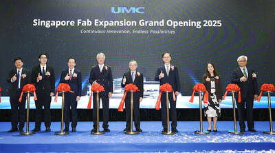
TIGHT-LIPPED: UMC said it had no merger plans at the moment, after Nikkei Asia reported that the firm and GlobalFoundries were considering restarting merger talks United Microelectronics Corp (UMC, 聯電), the world’s No. 4 contract chipmaker, yesterday launched a new US$5 billion 12-inch chip factory in Singapore as part of its latest effort to diversify its manufacturing footprint amid growing geopolitical risks. The new factory, adjacent to UMC’s existing Singapore fab in the Pasir Res Wafer Fab Park, is scheduled to enter volume production next year, utilizing mature 22-nanometer and 28-nanometer process technologies, UMC said in a statement. The company plans to invest US$5 billion during the first phase of the new fab, which would have an installed capacity of 30,000 12-inch wafers per month, it said. The

‘SWASTICAR’: Tesla CEO Elon Musk’s close association with Donald Trump has prompted opponents to brand him a ‘Nazi’ and resulted in a dramatic drop in sales Demonstrators descended on Tesla Inc dealerships across the US, and in Europe and Canada on Saturday to protest company chief Elon Musk, who has amassed extraordinary power as a top adviser to US President Donald Trump. Waving signs with messages such as “Musk is stealing our money” and “Reclaim our country,” the protests largely took place peacefully following fiery episodes of vandalism on Tesla vehicles, dealerships and other facilities in recent weeks that US officials have denounced as terrorism. Hundreds rallied on Saturday outside the Tesla dealership in Manhattan. Some blasted Musk, the world’s richest man, while others demanded the shuttering of his

Taiwan’s official purchasing managers’ index (PMI) last month rose 0.2 percentage points to 54.2, in a second consecutive month of expansion, thanks to front-loading demand intended to avoid potential US tariff hikes, the Chung-Hua Institution for Economic Research (CIER, 中華經濟研究院) said yesterday. While short-term demand appeared robust, uncertainties rose due to US President Donald Trump’s unpredictable trade policy, CIER president Lien Hsien-ming (連賢明) told a news conference in Taipei. Taiwan’s economy this year would be characterized by high-level fluctuations and the volatility would be wilder than most expect, Lien said Demand for electronics, particularly semiconductors, continues to benefit from US technology giants’ effort