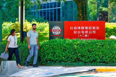
Taiwan Semiconductor Manufacturing Co (TSMC, 台積電), the world’s largest contract chipmaker, yesterday said it plans to raise capital expenditure to more than US$7 billion in an effort to satisfy customers’ strong demand for its advanced 28-nanometer chips.
That is an increase of about 17 percent on an estimate of US$6 billion that TSMC made three months ago.
TSMC’s move followed speculation that constraint in its supply of 28-nanometer chips had prompted clients Nvidia Inc and Qualcomm Inc to look for a second source, such as south Korea’s Samsung Electronics Co, United Microelectronics Co (UMC, 聯電) and Abu Dhabi-funded GlobalFoundries Inc, the contract chip manufacturer that was spun off from Advanced Micro Devices Inc in 2009.
“Yes, we have had some difficulties with 28-nanometer chips, but those difficulties had to do with not having enough capacity, not the yields,” a public relations official cited TSMC chairman and chief executive Morris Chang (張忠謀) as saying at a technology forum in San Jose, California.
The Hsinchu-based company expects to complete 132 tape-outs of 28-nanometer chips for customers this year after finishing 36 at the end of last year, Chang said in January.
In the semiconductor industry, tape-out refers to the final stage of the chip design cycle, before it is sent for manufacturing.
This year, 28-nanometer chips are expected to account for about 10 percent of the company’s total revenues, Chang said in January.
“In 2011, we spent US$7 billion [on new equipment]. This year, we will spend more than the US$7 billion we spent last year,” Chang told customers at yesterday’s forum in the US.
Chang said he would give a precise figure in a few weeks.
The increase in capital spending matched the expectations of Credit Suisse, which upgraded its forecast on TSMC’s capital spending to US$7 billion for this year, allowing the chipmaker to increase its 28-nanometer capacity to 50,000 wafers a month.
That would see 28-nanometer chips make up between 15 percent and 20 percent of TSMC’s revenues by the fourth quarter of this year, Credit Suisse said in a report dated April 10.
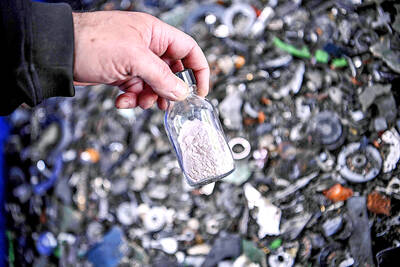
RECYCLE: Taiwan would aid manufacturers in refining rare earths from discarded appliances, which would fit the nation’s circular economy goals, minister Kung said Taiwan would work with the US and Japan on a proposed cooperation initiative in response to Beijing’s newly announced rare earth export curbs, Minister of Economic Affairs Kung Ming-hsin (龔明鑫) said yesterday. China last week announced new restrictions requiring companies to obtain export licenses if their products contain more than 0.1 percent of Chinese-origin rare earths by value. US Secretary of the Treasury Scott Bessent on Wednesday responded by saying that Beijing was “unreliable” in its rare earths exports, adding that the US would “neither be commanded, nor controlled” by China, several media outlets reported. Japanese Minister of Finance Katsunobu Kato yesterday also
‘DRAMATIC AND POSITIVE’: AI growth would be better than it previously forecast and would stay robust even if the Chinese market became inaccessible for customers, it said Taiwan Semiconductor Manufacturing Co (TSMC, 台積電) yesterday raised its full-year revenue growth outlook after posting record profit for last quarter, despite growing market concern about an artificial intelligence (AI) bubble. The company said it expects revenue to expand about 35 percent year-on-year, driven mainly by faster-than-expected demand for leading-edge chips for AI applications. The world’s biggest contract chipmaker in July projected that revenue this year would expand about 30 percent in US dollar terms. The company also slightly hiked its capital expenditure for this year to US$40 billion to US$42 billion, compared with US$38 billion to US$42 billion it set previously. “AI demand actually
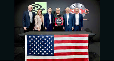
Jensen Huang (黃仁勳), founder and CEO of US-based artificial intelligence chip designer Nvidia Corp and Taiwan Semiconductor Manufacturing Co (TSMC, 台積電) on Friday celebrated the first Nvidia Blackwell wafer produced on US soil. Huang visited TSMC’s advanced wafer fab in the US state of Arizona and joined the Taiwanese chipmaker’s executives to witness the efforts to “build the infrastructure that powers the world’s AI factories, right here in America,” Nvidia said in a statement. At the event, Huang joined Y.L. Wang (王英郎), vice president of operations at TSMC, in signing their names on the Blackwell wafer to
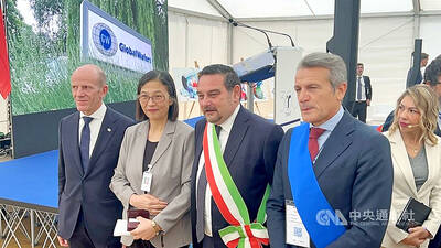
Taiwan-based GlobalWafers Co., the world’s third largest silicon wafer supplier, on Wednesday opened a 12-inch silicon wafer plant in Novara, northern Italy - the country’s most advanced silicon wafer facility to date. The new plant, coded “Fab300,” was launched by GlobalWafers’ Italian subsidiary MEMC Electronics Materials S.p.A at a ceremony attended by Taiwan’s representative to Italy Vincent Tsai (蔡允中), MEMC President Marco Sciamanna and Novara Mayor Alessandro Canelli. GlobalWafers Chairwoman Doris Hsu (徐秀蘭) said the investment marked a milestone in the company’s expansion in Europe, adding that the Novara plant will be powered entirely by renewable energy - a reflection of its